Kaohsiung courting TSMC’s first angstrom-scale facility: report
Kaohsiung courting TSMC’s first angstrom-scale facility: report
2024-08-12
Could TSMC be about to build its first angstrom-scale facility? According to Chinese-language media, Kaohsiung has proactively assessed its land availability and electricity supply, in order to court TSMC. Kaohsiung reportedly wants to host TSMC’s advanced 14-angstrom technology, which is equivalent to 0.14 nanometers. So far, TSMC has declined to comment on the market rumors.
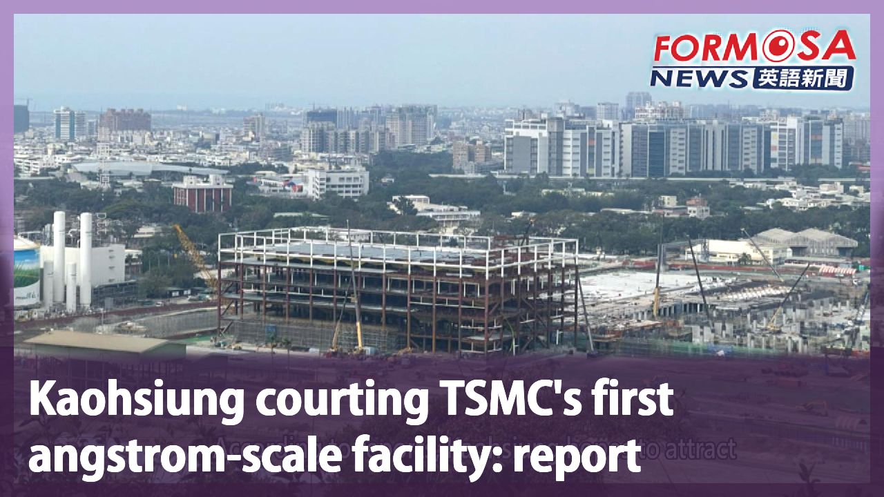
From Banpingshan, you can see the construction progress of TSMC’s Kaohsiung plant. The site will reportedly be the first to employ 2-nanometer technology. Completion is slated for the second half of the year, with 1,500 workers expected to move to Kaohsiung. Amid the global race to build smaller chips, Kaohsiung has rolled out the red carpet for top chip players like TSMC.
Chen Chi-mai (June 4)
Kaohsiung mayor
Companies that invest in Kaohsiung with advanced plants get bonuses such as three dock spaces. If you’re feeling down, you can set off to sea.
According to reports, Kaohsiung hopes to attract five semiconductor wafer plants. Mayor Chen Chi-mai has taken steps to ensure the city has enough water, electricity and land to accommodate them. He’s said there are two sites at Nanzi’s technology park that can house plants operating at the 2-nanometer level and below. Such plants would produce chips measured not in nanometers but in angstroms, or one-tenth of a nanometer. The chips’ finer circuitry would enable higher processing capabilities and data storage capacities.
Nobunaga Chai
Semiconductor industry analyst
They can be anti-dust and anti-bacterial. First, your client base needs to be large enough. Second, you need to have enough funds. Third, you need to have the technology. Among the world’s top and second-tier semiconductor firms, only three meet the criteria: TSMC, Samsung and Intel.
The battle for angstrom chips is on, and Taiwan’s local governments are competing to attract an advanced TSMC facility. The company has not addressed any rumors on the matter.
Nobunaga Chai
Semiconductor industry analyst
The machines that use extreme ultraviolet light consume a lot of electricity. And high-aperture extreme ultraviolet light requires even more electricity.
The cost of building a single 2-nanometer fab can hit US$20 billion, or about NT$600 billion. Experts say that fabs operating at the angstrom level face even bigger challenges, as they require a lot of electricity, highly skilled talent, and capital. If TSMC is to continue its Taiwan expansion, energy will remain an important issue to confront.
For more Taiwan news, tune in:
Sun to Fri at 9:30 pm on Channel 152
Tue to Sat at 1 am on Channel 53
台積電"埃米廠"會蓋在哪? 高市府超前部署鎖定"14A技術"
2024-08-12
晶圓代工技術已經從奈米,進入"埃米"之戰,台積電"埃米廠"落腳地點,備受關注!高雄市超前部署,盤點土地和水電,鎖定14A技術,也就是14埃米廠區,強調楠梓園區還有兩座基地可以容納設廠需求,市長陳其邁積極爭取,不過台積電對於市場傳聞,低調不回應。
從高雄半屏山,遠眺台積電高雄廠建廠進度,這傳出是二奈米第一座晶圓廠,有望今年下半年完工,1500人將陸續進駐高雄。隨著晶圓三雄"埃米戰爭"開打,高雄市不斷向台積電喊,選我選我。
[[高雄市長 陳其邁(06.04)]]
“來高雄的話,我們這些高雄投資的先進的廠商,我們都附送三個船席,心情不好可以出海”
日前傳出高雄喊出,蓋五座晶圓廠目標,市長陳其邁一步一腳印,盤點水電和土地,強調楠梓園區還有兩座基地,可以容納兩奈米以下設廠需求。先進製程"埃米",是一奈米的十分之一,電路越細,代表半導體的處理能力和數據儲存容量就越高。
[[資深產業分析師 柴煥欣]]
“因為它可以防塵,然後防細菌的一些附著等等。第一個你的客戶的規模要夠大,然後第二個的話,你要有足夠的資金,第三個你要有足夠的技術,遍觀目前全世界一線到二線的晶圓代工大廠的話,也就只有台積電、三星跟英特爾”
晶圓三雄的"埃米之戰",正式展開,台積電的先進製程廠區,各地方政府積極爭取。不過對於市場傳言,台積電低調不回應。
[[資深產業分析師 柴煥欣]]
“極紫外光的機台,本身就是一個非常吃電的,一個吃電怪獸,但是高孔徑極紫外光的話,那它的吃電的狀況會更加的嚴重”
而且光是1座2奈米廠造價就要兩百億美元,約6千億台幣,專家分析,要蓋埃米廠,電力和高階人才以及資金需求挑戰更大,台積電要根留台灣、並技術升級,能源問題恐怕得先面對。
更多新聞內容,請鎖定:
民視台灣台(152頻道)週日至週五晚上9:30
民視新聞台(53頻道)週二至週六凌晨1:00
Related News