TSMC’s Advanced Packaging Plant No. 7 in Chiayi set to become world’s largest
TSMC’s Advanced Packaging Plant No. 7 in Chiayi set to become world’s largest
2026-02-03
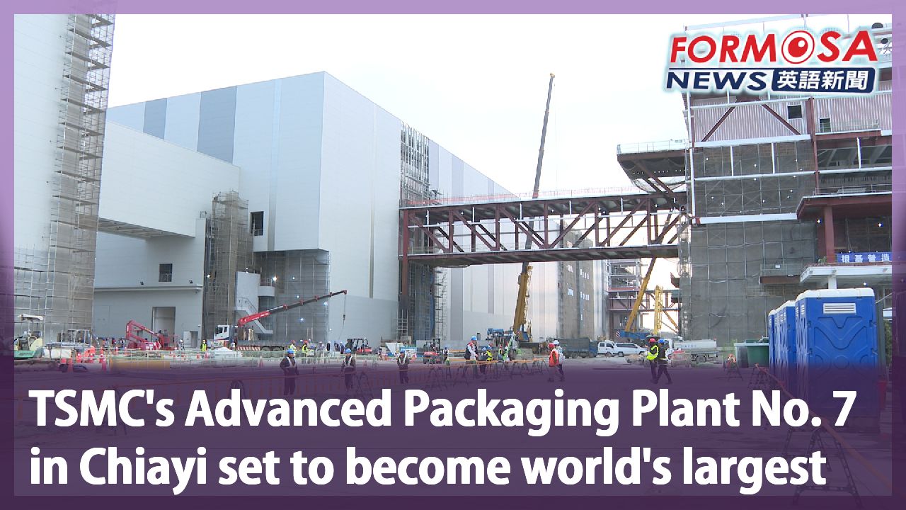
TSMC’s plans to expand in the US have divided public opinion, but it’s worth noting that the company’s investments in Taiwan are not decreasing. Today we’ll give you an inside look at construction of TSMC’s Advanced Packaging Plant No. 7 in Chiayi, revealed to the public for the first time. It’s expected to become the world’s largest advanced wafer packaging base in the future.
As we approach Chiayi’s High Speed Rail station, we can see huge factories and large-scale machinery towering over sugarcane fields in the distance. This is TSMC’s most advanced packaging plant, No. 7. Chiayi’s sugarcane fields are turning into fields of silicon.
Yang Ssu-min
FTV reporter
TSMC is showing us its Advanced Packaging Plant No. 7 in Chiayi for the first time. We can see that equipment is already being installed in the P1 section.
Workers carefully operate a forklift. The first phase of the plant’s construction began equipment installation last month. The second phase is still under construction. The two plants will have a total cleanroom area of 110,000 square meters, which is larger than 16 football fields. In the future, they are estimated to create 2,500 direct high-tech jobs.
Cliff Hou
TSMC Vice President
The AI boom means that global demand for semiconductor chips has increased significantly. Whether it is our advanced wafer manufacturing processes or packaging processes, our production capacity is distributed all over Taiwan and the projects we are building are increasing and accelerating.
Cheng Hsiu-jung
Southern Taiwan Science Park
Southern Taiwan has a very strong semiconductor corridor. Advanced packaging is also extremely important, so we are here today to declare that we value industrial safety here and want to ensure that construction can be completed smoothly.
There are 6,000 to 8,000 people working on site every day, rushing to get everything done, because demand for AI chips is high and production capacity is in short supply. However, last year, at the Chiayi packaging plant site, there were several reports of industrial safety accidents involving contractors. TSMC Chair C. C. Wei ordered a comprehensive strengthening of industrial safety measures.
Cliff Hou
TSMC Vice President
The challenges of new construction sites are greater and more numerous than those of older ones. Over the past six months, we have taken a different approach, with TSMC assuming direct management of the industrial safety committee.
TSMC has implemented six safety hazard training programs, requiring all workers to undergo training before entering the site. These programs utilize high-tech assistance to simulate hoisting and forklift operations, as well as scenarios involving falling objects from suspended loads and safety harness systems. The company is also collaborating with construction companies to establish the "Taiwan Semiconductor Construction Safety Association."
Yang Ssu-min
FTV reporter
The public is optimistic about the Chiayi site and there is room for expansion all the way up to a sixth phase at this plant. It’s expected to become the world’s largest advanced packaging plant. TSMC continues to increase its investments in domestic production capacity, using concrete actions to show its determination to keep its roots in Taiwan.
For more Taiwan news, tune in:
Mon to Fri at 9:30 pm on Channel 152
Tue to Sat at 1 am on Channel 53
#worldfirst #TSMC #Chiayitech
台積電持續投資台灣! 嘉義"封測七廠"首度曝光
2026-02-03
台積電擴大在美國設廠,引發關注,但實際上在台灣的投資並沒有減少。台積電位在嘉義的封測七廠,首度在鏡頭前曝光,目前已進行到第二期工程,未來有望成為全世界最大的先進封裝基地。
即將抵達高鐵嘉義站,遠方就能看到甘蔗田中,矗立著巨大廠房和大型機具,這裡就是台積電最先進的封測七廠,嘉義蔗田已成為矽田。
[[民視記者 楊思敏]]
“台積電首度曝光位在嘉義的先進封裝七廠,我們可以看到這個P1廠區,目前就已經在進行進機作業。”
人員小心操作堆高機,第一期廠房上個月已經進機,第二期興建中,兩個廠潔淨室面積,共11萬平方公尺,超過16座足球場大,未來提供2500個直接高科技工作機會。
[[台積電資深副總暨副共同營運長 侯永清]]
“AI的大潮流底下,全球對半導體晶片的需求大幅提升。不管是我們的先進晶圓製程,或者封裝製程,我們的產能在台灣各地,我們興建的工程在增加,在加速。”
[[南科管理局局長 鄭秀絨]]
“南台灣的半導體廊帶非常的強大。先進封裝也非常的重要,所以我們今天特別來宣示,我們重視這邊的工安,讓他們的建設可以順利地完成。”
現場每天都有6千到8千人作業,加緊趕工,就是因為AI晶片需求大,產能供不應求。然而,去年嘉義封裝廠工地,多次傳出包商工安意外,台積電董事長魏哲家下令,全面加強。
[[台積電資深副總暨副共同營運長 侯永清]]
“新的工地它的挑戰,是比舊的工地來的高和多。然後在過去6個月,其實我們做了一些不一樣的作為,工業安全委員會改為由台積電主動管理。”
台積電設置六項安全危害訓練,工人都要受訓才能進場,使用高科技輔助,模擬吊掛和堆高機作業,還有安全帶懸掛物體墜落的情境。公司也和營造廠商,要成立"台灣半導體營建工程安全協會"
[[民視記者 楊思敏]]
“外界看好嘉義這裡,後續還有擴充到六期廠房的空間,有望成為全球最大的先進封裝基地。台積電持續加碼投資國內產能,要以實際行動,展現根留台灣的決心。”
更多新聞內容,請鎖定:
民視台灣台(152頻道)週一至週五晚上9:30
民視新聞台(53頻道)週二至週六凌晨1:00
Related News